Plasma Jet Printing Technology
 Space Foundry
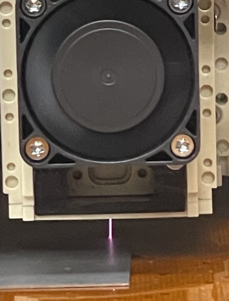
Space Foundry offers plasma jet printing technology for direct-write manufacturing of electronics on planar and complex 3D surfaces, including in-space manufacturing applications. They provide hardware configurations from desktop to industrial systems, as well as custom process development and print
Technical specifications
- Printing process
- Plasma jet printing (patented)
- Materials supported
- Conductive (copper, silver), Dielectric
- Surface types
- Planar, curved, vertical, complex 3D surfaces
- Pre/post-treatment
- Not required
- Adhesion
- Reliable adhesion via plasma activation
- Substrate compatibility
- Improved compatibility across multiple substrates
- Printing orientations
- Multiple orientations, including non-planar geometries
- Hardware configurations
- Desktop development systems, systems for non-planar printing, continuous printing for flexible substrates, robotic integrations, gantry integrations, industrial-scale systems
- Services offered
- Custom process/product development, printed service, feasibility studies, proof of concept projects
- Flight heritage
- NASA parabolic flight testing, connected to NASA programs and advanced aerospace applications
- Patent status
- Patent pending
About
Space Foundry’s patented plasma jet printing process enables direct-write manufacturing of conductive and dielectric materials without the need for separate pre-treatment or post-curing. The technology aerosolizes metal-ion inks, introduces them into a reactive plasma environment, performs in-situ reduction, and deposits conductive material directly onto the target surface in dry form. This allows for printing on curved, vertical, and complex 3D surfaces, supporting multiple orientations and challenging conventional additive methods. Plasma activation ensures reliable adhesion and improved compatibility across various substrates. The system supports copper, silver, and dielectric printing workflows for applications such as antennas, sensors, and related structures, replacing multi-step print, cure, align, and repeat cycles with a simpler direct-write approach.
The platform is designed for use cases where conventional additive methods struggle with curved surfaces, adhesion, orientation, thickness building, or process complexity. Applications include conformal antennas, frequency selective surfaces, electromagnetic shielding, and RF structures for aircraft, UAVs, missiles, and related platforms. It also supports electronics integrated into curved vehicle surfaces, such as LiDAR heaters and sensor structures. A key emerging use case is in-space manufacturing (ISM) of electronic components for both space and terrestrial applications, with the potential for in-space metallization. Other applications include printed sensors, EMI shielding, and communication features for robotic platforms and autonomous systems, and a future pathway for conformal electronics in sensors, monitoring devices, implants, and wearable systems.
Space Foundry offers multiple hardware configurations, including desktop development systems for R&D and process development, systems for printing on non-planar surfaces, continuous printing configurations for flexible substrates, and robotic and gantry integrations for large-format conformal printing. Industrial-scale systems are available for printing on large structures like aircraft surfaces and radomes. Beyond hardware, Space Foundry provides custom process/product development and printed services, allowing customers to leverage their expertise without capital equipment expenditure. They encourage feasibility studies and proof-of-concept projects for corporate R&D. The technology has been developed with support from NASA programs and advanced aerospace applications, with flight heritage demonstrated through parabolic flight testing.
Documentation
No public datasheet yet — request the datasheet / ICD from the supplier.