VLSI kit for low-power GLONASS / GPS navigation receiver
 Glavkosmos
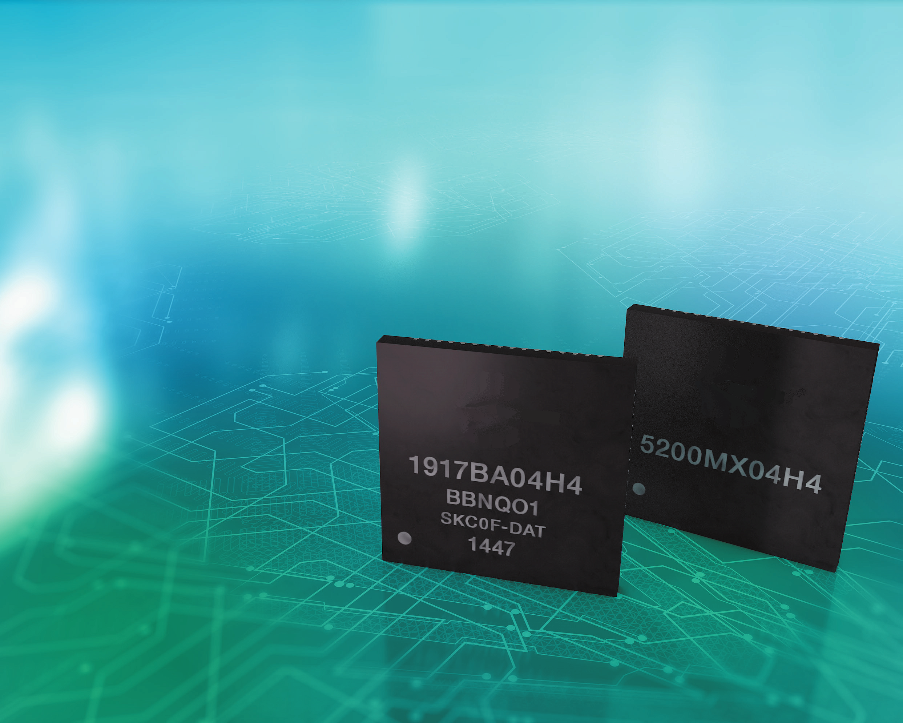
Two-chip low-power VLSI kit (VLSI 1 + VLSI 2) for multi-channel combined GLONASS/GPS navigation receivers.
Key figurescomparable across the catalogue
- Mass
- 0.001 kg
- Largest dimension
- 6 mm
- Design life
- 3 years
- Lead time
- 10 months
Normalised to common units so this product can be compared with others in its category. The supplier's own wording is below.
As published by the supplier
- Dimensions
- 6×6×1 mm
- Mass
- 1 g
- Supply voltage
- 1.20 ± 0.12 V (core); 1.8 ± 0.18 V (I/O)
- Operating temperature
- -40°C to +85°C
- Number of channels
- 36
- Frequency range
- L1 GPS C/A, L1 GLONASS ST/VT
- Battery power
- 1.6–3.6 V
- Active tracking consumption
- 0.07 W
- Processor frequency
- 60 MHz
- Design life
- 3 years
- Year of release
- 2015
- Production/delivery lead time
- 10 months
About
This VLSI kit is a two-chip solution for building low-power GLONASS/GPS navigation modules, released in 2015. VLSI 1 is designed for digital processing of signals from the GLONASS (L1 PT, VT) and GPS (L1 C/A) satellite navigation systems, solving the navigation problem in a multi-channel combined GLONASS/GPS receiver that includes a broadband linear path. VLSI 2 is designed for amplification, frequency conversion, filtering and digitization of signals from GLONASS (L1 VT) and GPS (L1 C/A), and is likewise used in a multi-channel combined GLONASS/GPS receiver. Each die measures just 6×6×1 mm and weighs 1 gram, with a 36-channel capability and an integrated processor clocked at 60 MHz. The kit runs on a 1.20 ± 0.12 V core supply and 1.8 ± 0.18 V I/O supply, with battery power input of 1.6–3.6 V, drawing only 0.07 W in active tracking mode. It operates across -40°C to +85°C. Glavkosmos guarantees a 3-year service life with a 10-month production and delivery lead time.
Documentation
No public datasheet yet — request the datasheet / ICD from the supplier.