PCI Express Chip 1888 BB 018 A
NTC Module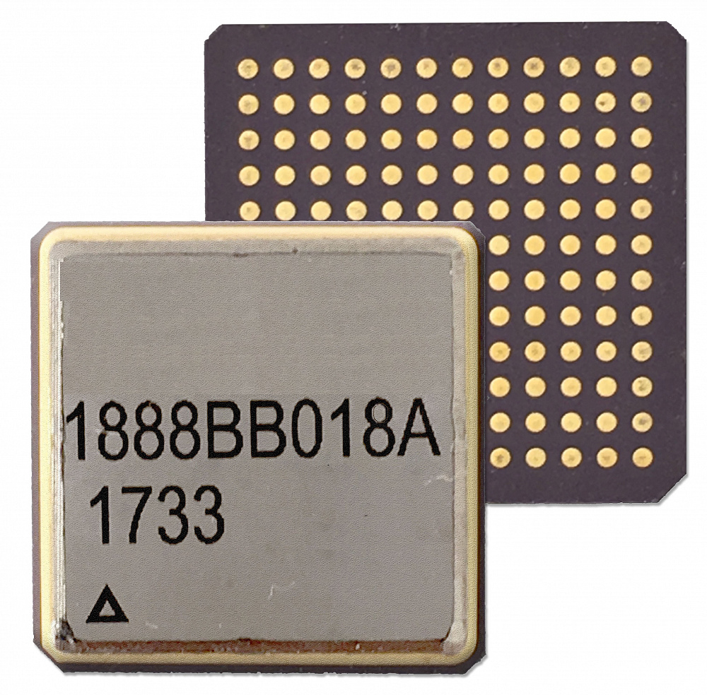
The 1888 BB 018 A is a PCI Express physical interface device chip designed to expand the functionality of interface modules and devices by supporting the high-speed PCI Express standard.
Key figurescomparable across the catalogue
- TRL
- 8
Normalised to common units so this product can be compared with others in its category. The supplier's own wording is below.
As published by the supplier
- Type of shell
- MK8306-144-1
- Supply voltage
- I / O buffers – 1.8 V to 3.3 V; cores: 1.25 V; I / O blocks: 1.2 V; clock generation circuits: 1.25 V; level offset circuits and calibration circuits: 3.3 V
- Dynamic current consumption for the power circuit
- UDDD1: 3.5 mA; UDDA2: 15 mA; UDDD2: 320 mA; UDDD3: 30 mA; UDDA1: 85 mA; UDD: 50 mA;
- Working temperature
- -60 +85 °C
- Technology
- CMOS 130 nm
- Type of acceptance
- 5
About
The PCI Express Chip 1888 BB 018 A is a microelectronic component developed to expand the functionality of various interface modules and devices. It achieves this by fully supporting the high-speed PCI Express standard, specifically adhering to the protocol and electrophysical interface requirements of the PCI Express™ Base Specification Revision 1.1. The chip is housed in a МК8306-144-1 shell and operates across a wide temperature range from -60°C to +85°C. It is manufactured using CMOS 130 nm technology. The chip features multiple supply voltage requirements for different internal components: I/O buffers require 1.8 V to 3.3 V, cores and clock generation circuits require 1.25 V, I/O blocks require 1.2 V, and level offset and calibration circuits require 3.3 V. Dynamic current consumption varies across different power circuits, including UDDD1 (3.5 mA), UDDA2 (15 mA), UDDD2 (320 mA), UDDD3 (30 mA), UDDA1 (85 mA), and UDD (50 mA). The product has a Type of acceptance classified as ‘5’.
Documentation
No public datasheet yet — request the datasheet / ICD from the supplier.